
TYPES OF EQUIPMENT
LITHOGRAPHY TOOLS
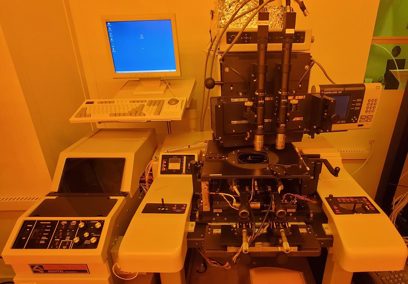
365 nm and 405 nm exposures at approximately 20 mW/cm2
Front side and backside alignment
Substrate geometries:
- 4" diameter
- 5" square
- 6" diameter
- good versatility on substrate thickness and geometry
Mask geometries:
- 5" square
- 7" square
- 9" square
- 1:1 copies of 5" substrate and mask
Print submicron features
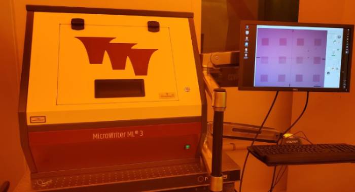
The MicroWriter ML3 Pro is a direct-write photolithography machine for rapid prototyping.
The ML3 Pro can write features down to 400nm into photoresists over a 195mm x 195mm x 15mm area.
Key Features:
- 195mm x 195mm maximum writing area
- 230mm x 230mm x15mm maximum wafer size
- 0.4µm, 0.6µm, 1µm, 2µm and 5µm minimum sizes across full writing area
- 365nm light source
- XY interferometer with 1nm resolution for precise motion control
- Writing speeds - up to: 17mm²/minute (0.6µm minimum feature size), 50mm²/minute ( 1µm minimum feature size),120mm²/minute (2µm minimum feature size) and 180mm²/minute ( 5µm minimum feature size)
- Auto focus system using yellow light with real-time surface tracking laser - no minimum wafer size
METROLOGY TOOLS
Electrical
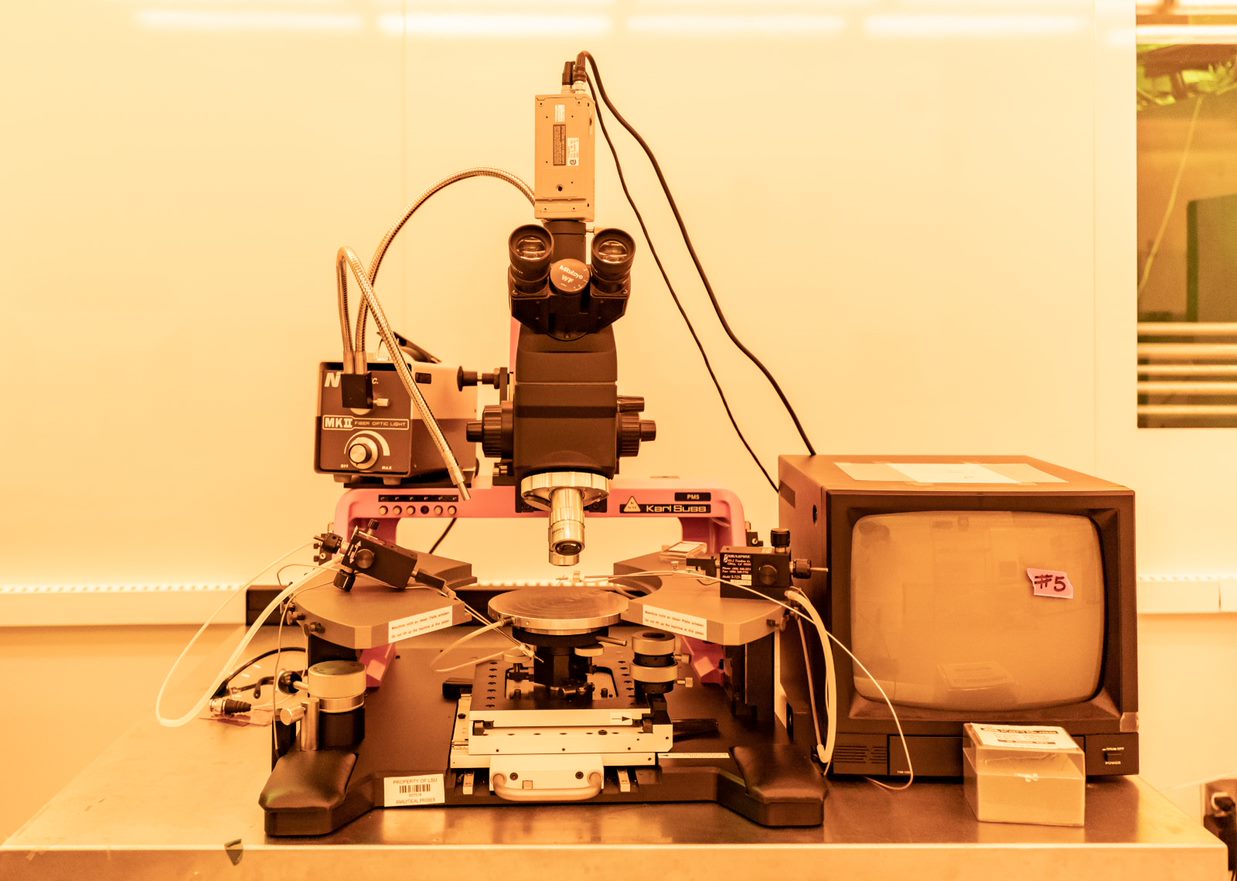
NFF refurbished Suss microprobe station updated to perform resist adhesion test. The apparatus is equipped with a 10 lb. linear motor, two microprobes, and a CCD camera for observation.
Capabilities:
- Capable of removing PMMA bonded sheets from Si
- Fine probing of microstructures
Optical
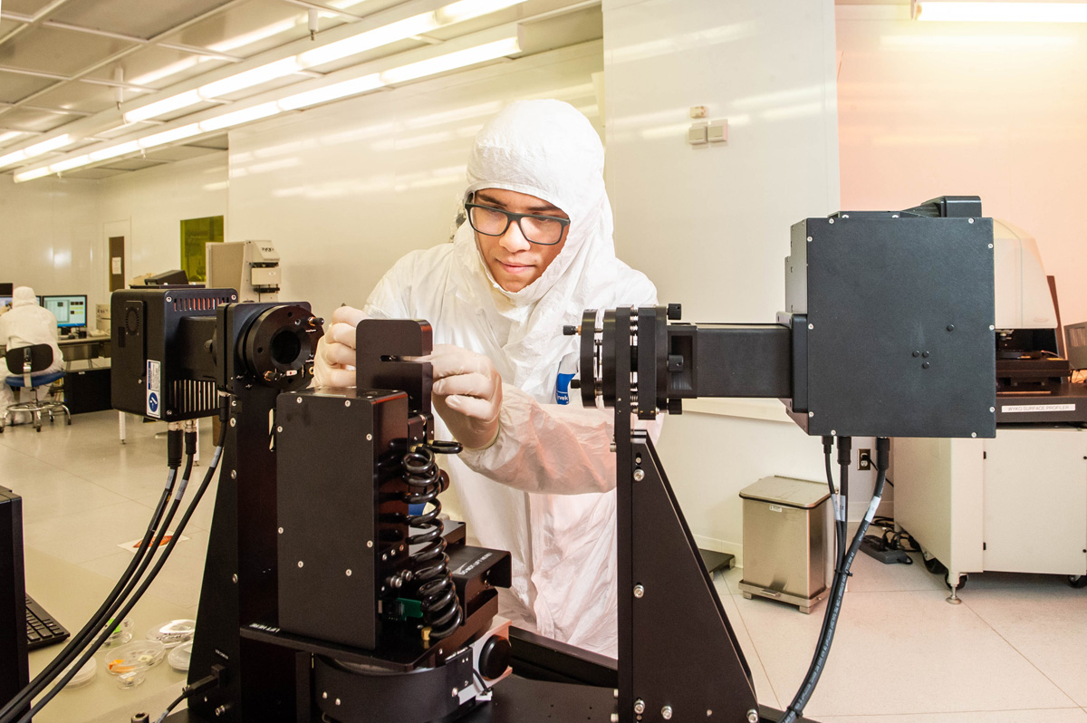
Ellipsometry measures the change in polarization as the polarized light interacts with the sample structure. The data is then analyzed to determine material properties like film thickness, optical constants, refractive index, etc. The RC2 ellipsometer is a tool with a unique capability of collecting all 16 elements of the Mueller matrix. Mueller matrix SE allows characterization of the most advanced samples and nanostructures.
Contact the assistant director, Sergi Lendinez for additional information and measurement services request
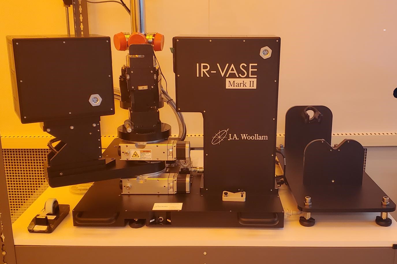
The IR -VASE is a spectroscopic ellipsometer that combines the chemical sensitivity of FTIR spectroscopy with thin film sensitivity of spectroscopic ellipsometry.
This tool covers a wide spectral range from
1.7um - 30um (333 cm -¹ - 5900 cm -¹)
Features:
- High Sensitivity to Ultra-Thin Films
- Non-Destructive Characterization
- No Baseline or Reference Sample Required
- Temperature range: 77K - 350°C
Contact the assistant director, Sergi Lendinez for additional information and measurement services request
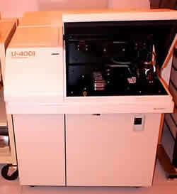
This U-4001 Spectrophotometer has equipped with a built-in 60mm Integrating Sphere and a optical table, and a 45-Degree Specular Reflectance Attachment(Absolute<) for solid samples(thin film/lens/wafer/solar cell/new material inspections) in the Transmittance and the Reflectance Measurements. Spectral Range: 175 nm~2,600nm (Direct Detection) or Integrating Sphere: 240nm~2,600nm region
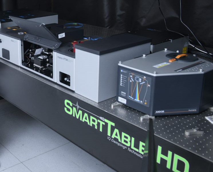
The neaSpec scattering-type Scanning Near-Field Optical Microscope (s-SNOM) combines advanced nanoscale imaging and spectroscopy in a single tool. The versatility of this microscope enables complete characterization of a large range of materials from polymers, biological samples, 2D materials, semiconductors and photonic devices
Customized specifications include:
- Visible (VIS, 633nm) laser source
- IR source (near and mid-IR ranging from 1.55um - 10um wavelengths
- Pulsed-pump @ 1.55um
Photoluminescence (PL) Spectroscopy and nano-imaging - Tip enhanced Raman Spectroscopy (TERS)
- Nano-FTIR (Fourier Transform Infrared Spectroscopy)
- Ultrafast pump-probe nanoscopy with fs resolution down to 10nm spatial resolution
Other features:
- Advanced AFM: tapping mode, Kelvin and conductive AFM, etc.
- Near-field amplitude and phase resolved microscopy at VIS, near and mid-IR ranges
- Wide spectral bandwith nano-FTIR @ mid-IR
- Ultrafast pump-probe microscopy with a 1.55um pump
- TERS at the nanoscale
Contact Sergi Lendinez for further information
| Range | Verticle Resolution | |
|---|---|---|
| PSI | up to 150 nm | 3 Ǻ |
| VSI |
up to 2mm | 3 nm |
For training or questions, please contact Sergi Lendinez
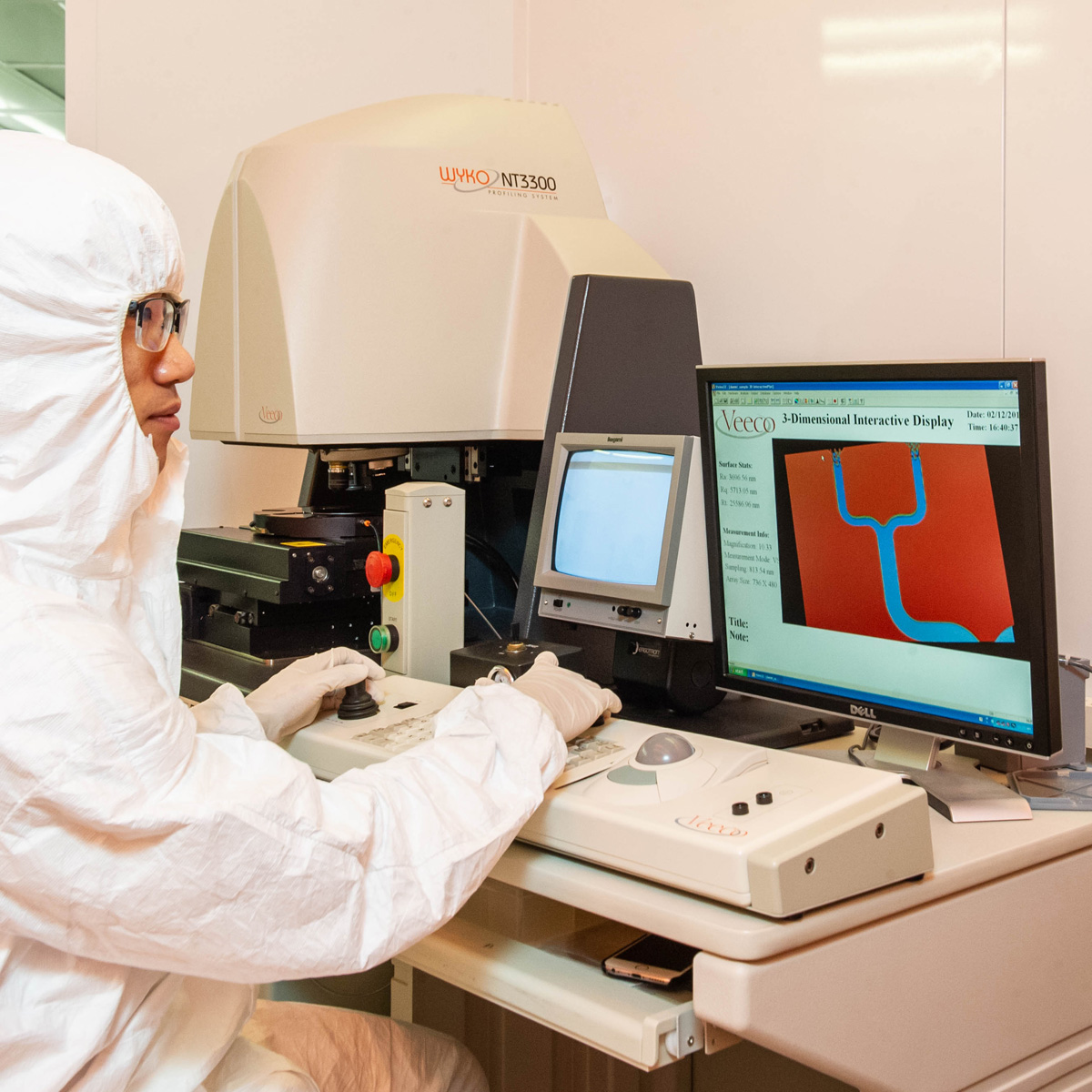
WYKO NT3300
The Optical Profiler investigates variations in topography for surfaces ranging from
very smooth to 2mm step height. Basic interferometric principles are used with light
reflected from a reference mirror combined with light reflected from a sample to produce
interference fringes, where the best-contrast fringe occurs at best focus.
Two modes of interferometry are used: PSI (Phase Shifting Interferometry) mode uses variations in phase of a monochromatic (632 nm) reference source to combine with beam reflected from the sample to form interference rings. The variation in intensity of the rings at significant phases is used to calculate small height variations on the sample surface. VSI (Vertical Scanning Interferometry) mode uses short coherence length of white light to measure the resulting degree of fringe modulation, or coherence, between the reference and sample beams as the interferometric objective moves vertically through sample focus. The vertical position of the optics at peak fringe contrast is extracted for each point on the sample surface, resulting in a topographical map.
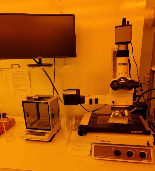
Capabilities:
- 2.5x, 5x, 10x and 20x magnifications
- CCD Camera
Laptop connection specs:
- image processing
- measurement
- save and export images
Electron Beam
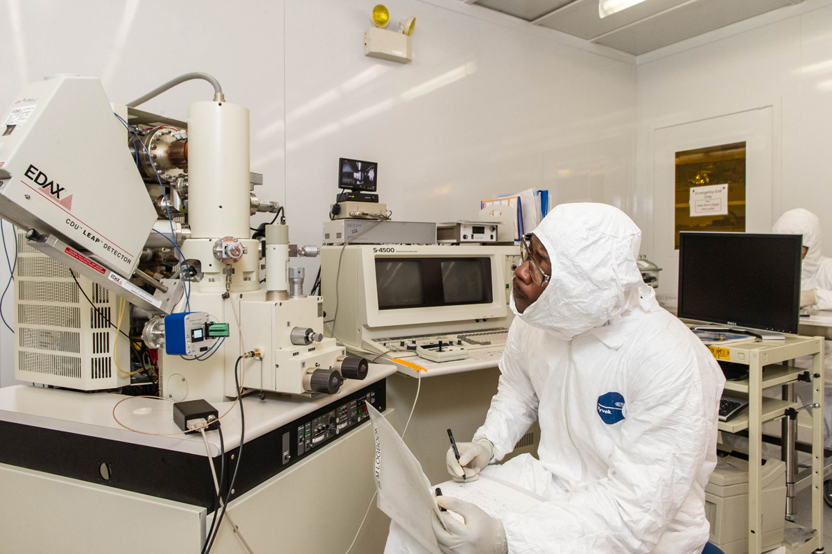
Hitachi S-4500 II Cold Field Emission Scanning Electron Microscope
This FE SEM is used to image features at magnification ranging from 20x to 500,000x.
Resolution depends on operating conditions:
- 1.5 nm (at 15 kV accelerating voltage, WD 4 mm)
- 4.0 nm (at 1kv accelerating voltage, WD 3mm).
Accelerating voltage can vary continuously from 0.5 kV for resist imaging to 30 kV for EDS detection and metallic surface imaging.
Stage motion ranges:
- X: 0 to 100 mm
- Y: 0 to 50 mm
- Z: 3 to 28 mm (continuous)
- Tilt: -5º to +45º
- Rotation: 360º (continuous)
Scan Probe
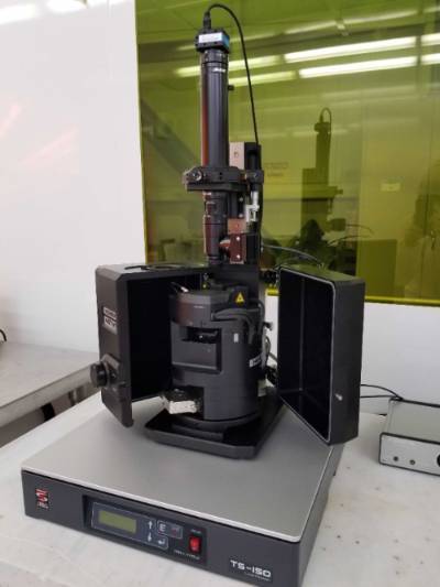
The Horiba SmartSPM Scanning Probe Microscope is a fully automated system that offers ultra-fast and high-resolution measurements for the most advanced materials research at the nano scale in all AFM modesT
Key Features:
- High speed 100µm scanner
- 1300nm AFM laser
- Lowest noise closed loop sensors
Operating Modes:
- Contact and Non-contact AFM mode in air/liquid
- Conductive AFM
- Kelvin Probe (Surface Potential Microscopy)
- Nanolithography
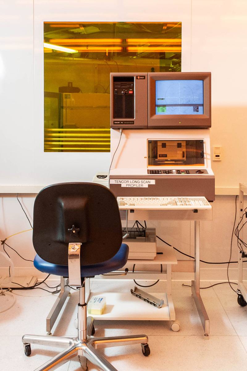
The Tencor Profiler is a metrology tool that generates a 2 dimensional profile of the surface of a sample. This is done by a stylus, which touches the surface of a sample and is scanned across a prescribed length. Step heights and widths of structure can be measured in this way. Measurement of vertical features ranging from under 100 Å (0.4 µin) to approximately 0.3 mm (11 mils), with a vertical resolution of 1 or 25 Å (0.004 or 0.1 µin)
Contact Sergi Lendinez for more details.
X-Ray
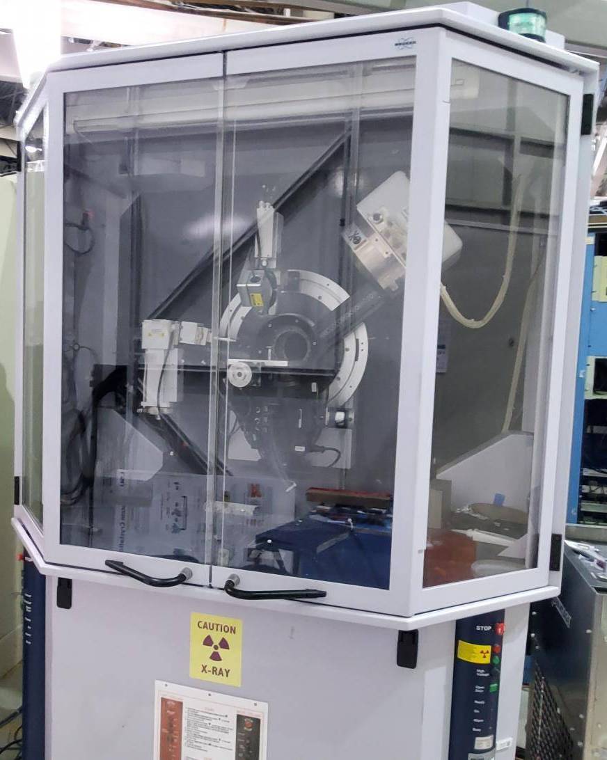
Bruker D8 is a multi-purpose diffractometer designed for the structural characterization of the full range of materials from powders, amorphous and polycrystalline materials to epitaxial multi - layered thin films at ambient and non-ambient conditions.
Features:
- Generate area detector for 2D diffraction measurements
- Phase Identification and quantification, structure determination and refinement, microstrain and crystallite size analysis
Contact Sergi Lendinez for more information and training
PROCESSING TOOLS
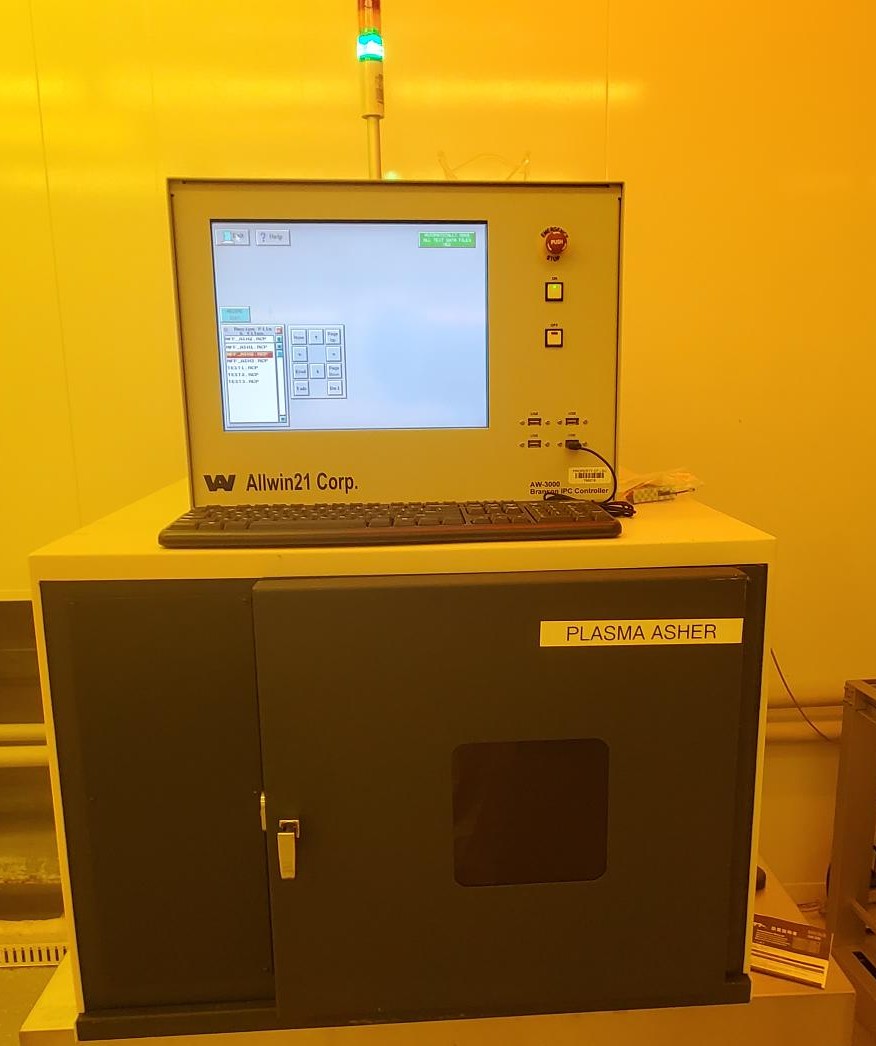
An O2 RF plasma can be used at CAMD to strip one to five microns of resist from up to 6 four inch wafers at a time.
Minor modification – The Bransen Plasma Asher reduced Nitrogen purge flow for the safe ashing of thin fragile membranes
Features:
- 1500 W 13.56 MHz RF generator
- Thermal probe
- Automatic processing
- Capable of processing with up to three gases ( O2 and N2 installed)
Capabilities
- Reactive ion etching with O2
Applications
- Resist stripping
- Substrate cleaning
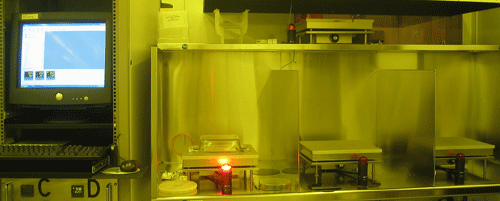
The hot plate station is comprised of four Prazitherm precision hot plates manufactured for resist processing. Each hot plate is sized 350mm x 350mm. They are flat and level, with temperature uniformity of +/- 0.5º. The maximum operating temperature is limited to 200ºC in order to maintain temperature inside the cleanroom. A hood located over the hot plate station ensures evaporated fumes are not released into the cleanroom environment.
Each hot plate is controlled through its own PID controller with a PC using iTools© software by Eurotherm. The programmable software allows for controlled and automated heating and cooling cycles, though there is no active cooling associated with the hot plates. Each controller has 4 recipes, with 16 segments available for programming each recipe.
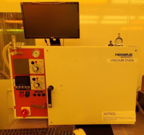
The Heraeus vacuum oven is controlled by a Delta DTP - PID controller. The controller is optionally PC interfaced for recipe storage and remote control or continuous heating. Temperture control is ± 0.5 degrees C
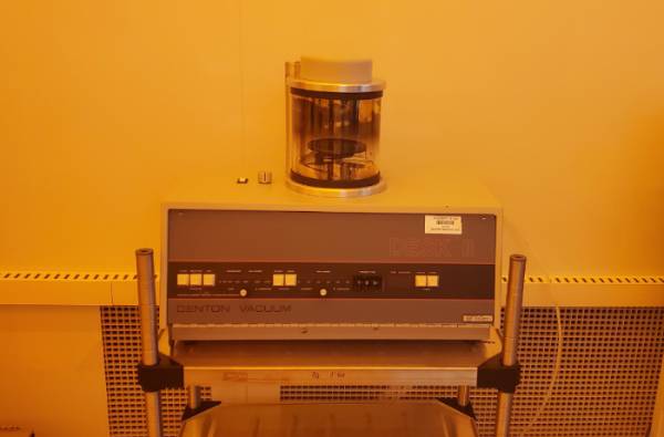
The Denton Desk II sputter coater is used to prepare SEM samples for imaging This machine sputters a thin layer of gold onto a substrate for the use of imaging with the SEM or collecting data on the Optical Profiler
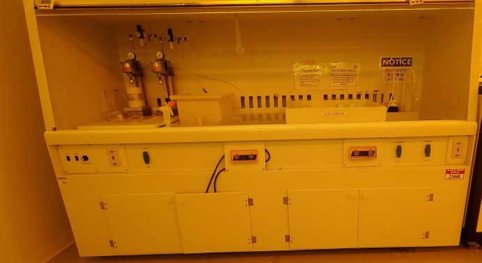
Equipped with sink, DI water, nitrogen guns and UV light protection, this hood serves as the primary station for the use of acids, etch processes and other corrosive chemicals
.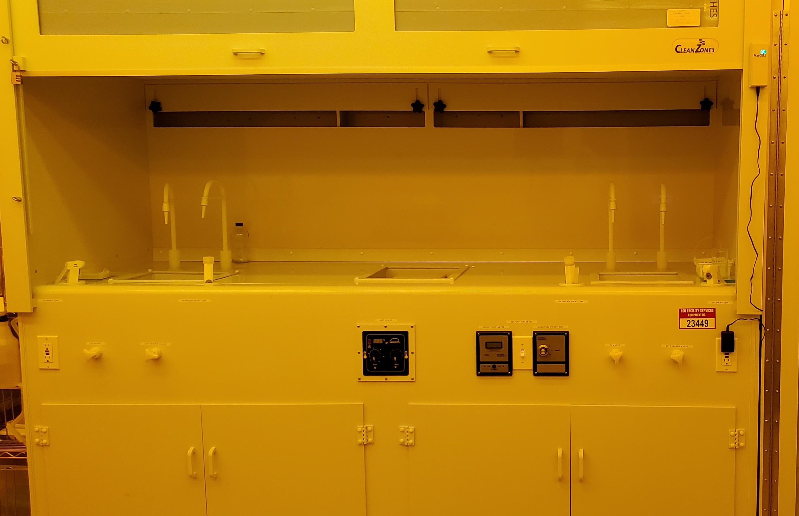
Equipped with two sinks, nitrogen guns, DI water, city water, hotplate and resistivity meter, this hood serves as the primary developing station. Hood is also equipped with UV light protection and is designed to provide ultra pure air flow
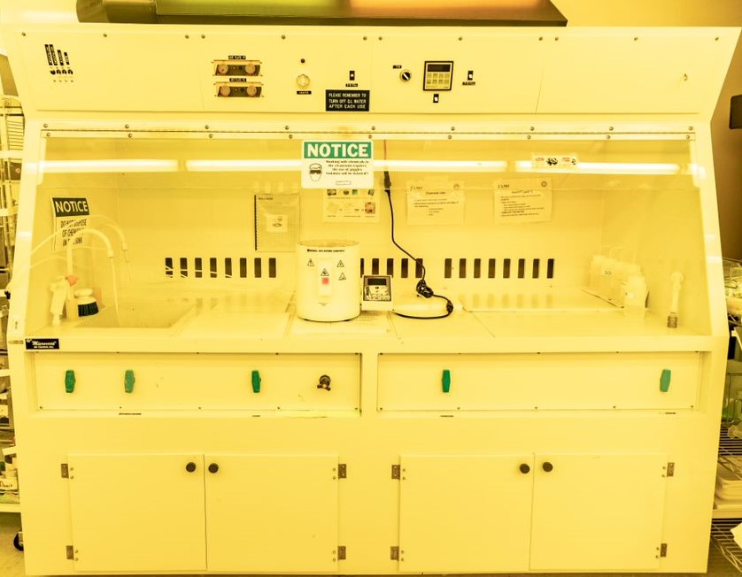
Equipped with sink, DI water, city water and nitrogen guns, this hood serves as the primary station for spincoating and cleaning processes
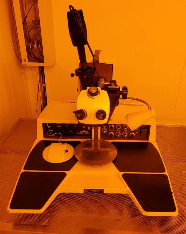
The K&S 4123 is an Aluminum and Gold wire wedge bonder that is used for bonding devices ranging from simple ICs and discrete devices up to complex hybrids with height variations up to 200 mil (5mm). The machine can operate in either thermosonic or ultrasonic mode.
Contact Sergi Lendinez for more information
DEPOSITION TOOLS
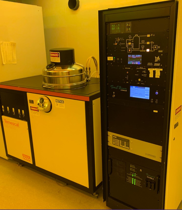
The Temescal E-Beam Evaporator allows deposition of metals and other materials on up to four wafers, (4 inch size) simultaneously.
Features:
- Multi-layer films with automatic precise rate control enabled by new controllers
- Base pressures in the mid 10-8 Torr
- New Dry and Cryo pumps for rapid pump down
- (4) pockets, allowing evaporation of multiple materials in a single run
- Deposition Materials: Al, Cr, Cu,Ti, Ni, In, *Au and *Pt (* materials charged separately according to market value )
- NOTE: materials pricing subject to change according to market value
Contact Sergi Lendinez for further information
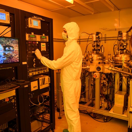
The Kurt Lesker CMS-18 sputtering system is composed of two independent chambers with a shared load-lock enabling versatile film depositions.
Key Features:
- Customizable automatic deposition recipes
- (3) deposition guns on each chamber
- Dedicated chambers for metals and insulators to reduce cross - contamination
- RF and DC magnetron sputtering
- Substrate RF bias
- Substrate heating up to 800°C
- Up to (3) process gases, allowing reactive sputtering
Contact Sergi Lendinez for more information